
DIP vs SMD vs COB
1. LED Display Packaging Device Development History:
LED package structure can be changed according to the needs of the application products, led chips can be made into different structure and appearance of the package devices through a variety of packaging methods, according to the packaging form of led display commonly used devices are mainly divide:
- 1). DIP
- 2). Dot Matrix Package
Dot matrix package is several led chips regularly arranged in a matrix of 4 × 4 or 8 × 8, etc. glued and soldered on a micro-PCB board, using a plastic reflective frame cover and potting epoxy resin, the outer leads are mostly connected to the internal micro-PCB using a double row of steel pins. Because of its full wrapping package, its internal structure is stable and protective.
- 3). In-line Three-in-one Package
Through the improvement of the straight plug process, the three RGB chips are sealed into one straight plug light, and the outdoor three-in-one product is developed. It does not change the packaging process of traditional straight plug light, but breakthrough in the product structure and combination by sealing RGB in one light and using four light pins. Using this packaging method, the inline led display can achieve a smaller density without changing the production process and is very competitive in price.
- 4). SMD
- 5). COB
From the development history of packaging methods, each transformation is a technical innovation, but also a reflection of led enterprises in pursuit of innovation and better display effects. SMD products in the continuous progress of technology, in terms of chromaticity and protection level has made great progress, SMD in the outdoor applications are becoming more and more widespread; COB package of many advantages, led display companies will COB package reference to small pitch led display.
- 6). Micro LED

2. DIP:
- 1). What Is DIP package?
DIP package is the abbreviation of dual inline-pin package, commonly known as plug-in lamp type, is the earliest used; led lamp (led display commonly used are F546 and F346) inserted into a special PCB board, after wave soldering to produce semi-outdoor module and outdoor waterproof module.
Initially, three colors of red, green, and blue lamps are inserted into the PCB to form an RGB pixel, and later it has been possible to package three kinds of RGB chips in one lamp bead, that is, three-in-one outdoor full-color screen, which has relatively improved the production efficiency and production cost.
But whether single RGB or three-in-one RGB there are point spacing is limited by the diameter of the lamp beads, currently can only do P6, the other P5, P4 or even higher density outdoor led display, cannot be made.
The production of DIP packaging method, not easy to mechanize production, low production efficiency, no high technology and equipment threshold. The protection performance of the direct plug is good, but the perspective is not good for precise fixing, generally between 100-110, and high energy consumption, not environmentally friendly, so only suitable for outdoor, currently in the outdoor P8-P20 and a larger market share.
- 2). Advantages of DIP
DIP as the main force of the led display over the past in the industry it still retains its place in the led display industry with its comparative advantage over the performance of outdoor surface. DIP is still the best choice for making screens, especially in the field of large screens, or some special applications.
A. Single lamp: DIP lamp, it has a build-in single-color chip. Each of the three different colors of red, green, and blue is assembled to form one pixel of the full-color display. With only one wick wrapped in each lamp and log lamp foot so that it can easily achieve the ultra-high brightness required by the outdoor usage and it does not need to increase the current to increase the brightness, then the heat dissipation is not a problem. The chip of DIP is packaged separately, and it got high brightness, small driving current, good heat dissipation, low failure rate and low attenuation rate.
B. Way of soldering: The pins of the DIP lamp are soldered after soldering through the PCB board, then the soldering of the DIP is much stronger. The solder joint issue does not easily come up during transportation or using especially in the relatively harsh outdoor environment, thus the maintenance failure rate is low to achieve the purpose of reducing the daily cost, so ensuring the welding quality is one of the key factors to ensure the quality of the outdoor display.
C. DIP LEDs contain two connecting pins which are mounted through-hole to PCBs (printed circuit boards). DIP LEDs have higher optical decay, lower CRI, and lower efficiency than the more recent SMD LEDs. However, many DIPs are used in larger pixel pitch outdoor led screens to achieve higher brightness.
• 3). DIP or Dual Inline Plane LEDs are individual red, green and blue diodes that together can make white or any other color. Due to their larger size, DIP LEDs are brighter than SMD.
In the United States, most fixed installation displays are sold with a 5-year warranty. The display is expected to stay color matched and bright during this period. With SMD, the display is less bright from day 1, and only continues to get dimmer over the life of the display.
For DIP displays, the DIP346 found in P10 displays is priced to move. This is a well-tested product, and the resolution is high enough for most applications. DIP546 is used for special applications such as scoreboards and traffic signs. The standard viewing angle of a DIP led display is 110°(H)/60°(V) while an SMD Display is 160°(H)/120°(V).
DIP Use for outdoor led screen: P8, P10, P16, P20.

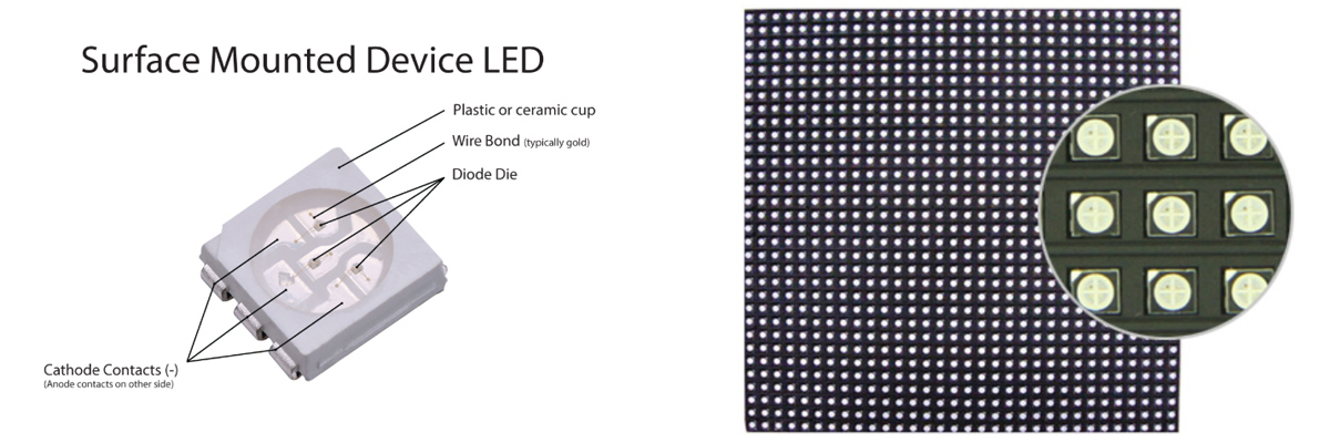
3. SMD:
- 1). What Is SMD Display?
SMD package, is the abbreviation of Surface Mounted Devices, meaning surface mount devices, it is SMT (Surface Mount Technology Chinese: surface adhesion technology) components in a kind of. After the electronic circuit board automated production machine is introduced, some simple pin components can be placed on the PCB for wave over soldering fixed.
Surface mount components were introduced about twenty years ago and thus ushered in a new era. Everything from passive components to active components and integrated circuits eventually became surface mount devices (SMD) and could be assembled by equipment. For a long time, it was believed that all pin components could eventually be packaged in SMD packages, and since then SMD technology has been widely used in led displays.
- 2). Core Materials of SMD Process
A. Bracket: Conductive, support and heat dissipation, mostly for the bracket material after plating and formed, from the inside to the outside of the material, copper, nickel, copper, silver, which is composed of five layers.
B. LED chip: Chip is the main component of the led lamp material, is the light-emitting semiconductor material.
C. Conductive wire: connect the wafer PAD (solder pad) and the bracket and enable it to conduct.
D. Epoxy resin: Protects the internal structure of the lamp beads, and can slightly change the light-emitting color, brightness, and angle of the lamp beads.
- 3). Advantages of SMD
Three-in-one is a kind of SMD technology for led display, which means that the SMT lights packaged with three different colors of RGB led wafers are packaged in the same gel according to a certain spacing.
A. The whole screen perspective is relatively DIP larger, and the surface can do light diffuse reflection processing, the resulting effect is not granular, good color uniformity.
B. In terms of color, the three-in-one full color splitting and color separation is easier than the three-split one, and the color saturation is high.
C. With the whole surface to light, so the overall color of the three-in-one more uniform, flatness is easier to control.
D. SMD LEDs are the more recent, resilient, efficient, and long-lasting technology for mass production.
E. SMD parts can be made smaller and thinner because the part is only soldered to the “surface” of one side of the circuit board.
F. SMD screens usually use 3-in-1 LEDs. With one RGB 3-in1 led unit per pixel, there are three tiny led chips sealed inside a single part. Therefore, the color blends better, and the image is sharper.
- 4). SMD Disadvantages
The early development, because of the complex manufacturing process, maintenance difficulties, resulting in very high costs, generally used in high-end led display products. In recent years, due to the rapid development of technology and continuous improvement of the production process, many automatic equipment, SMD has developed rapidly, the cost has been reduced a lot, is now the mainstream of led indoor display products.
And has begun to penetrate the outdoor display market, but the brightness and outdoor waterproof, moisture-proof, dustproof, anti-static, anti-oxidation has been its insurmountable chasm.
SMD small pitch is generally the led lamp beads exposed, or the use of mask. Due to the characteristics of mature and stable technology, low manufacturing cost, good heat dissipation and easy maintenance, it also occupies a large share in the led application market. But due to the existence of serious defects, is no longer able to meet the needs of the current market.
A. Low protection level: Does not have moisture-proof, waterproof, dustproof, shockproof, anti-collision. In a humid climate, it is easy to have large batches of dead and bad lights. In the process of transportation, it is easy to drop the lights and bad lights. Also, easy to be affected by static electricity, causing the phenomenon of dead lights.
B. Eye damage: Long time viewing will appear blinding, fatigue, cannot protect the eyes. In addition, there is a “blue harm” impact, because the blue led wavelength is short, high frequency, the human eye directly, long-term exposure to blue light, easy to cause retinopathy.
C. LED lamp life is short: Lamp performance by environmental factors, the service life is greatly shortened, PCB performance by environmental factors, copper ion migration, resulting in micro-short circuit.
D. Mask: SMD small pitch using mask, when used in high temperature environment, the mask is prone to bulge, which affects the viewing. After a period of use, the mask cannot be cleaned, resulting in whitening or yellowing site occurred, not only the appearance of unsightly, but also affect the viewing.
• 5). For rental installations, SMD is the clear choice; the numbers represent the package size, so SMD3535 would be 3.5mm x 3.5mm and SMD2727 would be 2.7mm x 2.7mm; choose the right SMD, when it comes to SMD’s, there are a lot of choices:
Nationstar gold wire, Nationstar copper wire, Kinglight, Kn-light, Hongsheng, Mulinsen, Miyou, Multi-color……
Indoor LED Screen:
SMD1010: P1.25, P1.56, P1.875
SMD1515: P1.875, P2, P2.5, P2.604, P2.98
SMD2020: P2.5, P3.076, P3.91, P4, P4.81
SMD2121: P3, P3.91, P4, P4.81, P5, P6
Outdoor LED Screen:
SMD1415: P2.5, P2.6, P2.98
SMD1921: P3, P3.91, P4, P4.81, P5, P5.33
SMD2525: P5, P6
SMD2727: P5.95, P6, P6.67
SMD3535: P6, P6.25, P6.67, P8, P10

4. COB:
- 1). What is COB?
COB package is the abbreviation of English: Chip on Board, which directly translates to chip on board. In the field of led display technology, COB packaging process is to fix the led bare crystal chip with conductive adhesive or insulating adhesive on the PCB light position pads, and then use ultrasonic welding technology to conductive function of the led chip lead welding together, and finally use epoxy resin adhesive to encapsulate the light position to protect the light-emitting chip.
If the bare chip is directly exposed to air, it is vulnerable to pollution or human damage, which affects or destroys the chip function, so the chip and bonding leads are encapsulated with adhesive. It is a new packaging method that is different from DIP and SMD packaging technology. Compared with DIP and SMD, it is characterized by space saving, simplified packaging operation and highly efficient thermal management method. It has certain advantages in terms of manufacturing efficiency, low thermal resistance, optical quality, application, and cost.
Newer COB technology presents many advantages: wide viewing angle, solid dustproof, shockproof, and often waterproof surface which is rigid and prevents damage to led elements. Flat and even face minimizes more effect.
- 2). Advantages of COB Packaging Process:
A. High reliability: An important indicator to evaluate the reliability is the dead light rate. LED display industry currently uses the national standard is: three ten thousandths; COB packaging process can now make the indicator to. Full-color screen: less than five hundred thousandths. Single, two-color screen: less than eight parts per million.
Why COB package display has such high reliability, we analyze through the following five aspects:
a). Single lamp production process control link reduction: a full-color lamp beads need five solder lines, from the point of view of the production of lamp beads, COB packaging process only need to control the quality of these five solder lines in the production process, while the SMD packaging process in addition to the quality of these five solder lines to control, but also need to control the quality of the four solder pins of the lamp beads face over the reflow process bracket welding, according to the principle of reliability, a system of COB and SMD control links are 5 and 9, so COB reliability in this regard is at least nearly twice as high as SMD.
Taking a square meter of led display as a unit, if the production of 1 square meter of P10, COB packaging process will save 40,000 control points. If the point density is reduced by a factor of two, that is, the point density to P5 level, COB packaging process per square meter to save 160,000 solder joints. If the dot density is further reduced to P2.0 level, the COB packaging process will save 1 million solder joints per square meter.
If the point density of P1.0 level, COB packaging process will save 4 million solder joints. On the contrary, the SMD package how to ensure that these millions of solder joints do not appear false, continuous solder, false solder, is a major headache. COB packaging process has created a revolutionary step to get rid of the bracket surface paste welding this link. This is one of the highest weighted factors to ensure the high reliability of COB package.
b). COB package eliminates the bead surface over the reflow process, no longer cause the traditional packaging process reflow oven high temperature on the led chip and solder line failure.
Reflow oven will generally have a high temperature of 240 °. If the epoxy resin adhesive TG point is too low, or the packaging process has moisture inhalation, high temperature will lead to non-linear rapid expansion of the colloid, resulting in the led chip solder line pull off damage failure. In addition, high temperature will be through the bracket pin will quickly conduct heat to the chip, resulting in the chip body cracking shattering the possibility of increased failure. And this problem is the most terrible, generally in the factory aging test will not be a problem, after transport to the client and then use a period, the problem will be gradually exposed.
c). Good heat dissipation: COB packaging process is to directly fix the led bare chip to the pad, so the heat dissipation area is relatively large compared to the traditional packaging process, the material comprehensive heat transfer coefficient is also high, good heat dissipation. The traditional package is to fix the led bare chip on the pad inside the bracket, and the pad needs to indirectly transfer the heat to the PCB board through the metal pin of the bracket.
d). Immersion gold PCB board process: COB package process circuit board using immersed gold process, not using the traditional package usually used PCB board spray tin process, so in outdoor application conditions, live in the hot and humid environment and salt spray application conditions, PCB board lines high oxidation resistance.
e). Outdoor protective treatment process without dead ends: COB packaging process lamp surface curve is smoothly rounded hemispherical surface, all devices on the lamp surface are sealed by epoxy resin adhesive, no device pin exposed outside. Therefore, no matter it is applied in indoor, outdoor environment or harsh humidity and salt fog environment, there is no worry about the oxidation of device pins causing lamp bead failure.
SMD package surface is not smooth and smooth over the curve, there will be a lot of raised quadrilateral blocks, quadrilateral fast and obvious angles. The exposed pins of the lamp bead surface need to be protected by outdoor protection treatment.
COB package in fact only need to the bead surface of the PCB and driver IC surface of the PCB and devices for nano-coating, anti-UV coating and three-proof paint spraying outdoor protection treatment, the treatment area does not exist any shadow area, no treatment dead ends. SMD package in the processing of surface mount lamp beads four legs or six legs of outdoor protection, in how to deal with the millions of solder joints of the antioxidant capacity will face another huge challenge.

B. Cost Savings
a). Save the cost of raw materials, COB package no longer uses metal raw materials such as brackets and braided tape.
b). Save process cost, COB package saves the cost of cutting, dividing, braiding and reflow soldering of lamp surface of lamp bead circuit board.
c). Save the transportation cost, COB package no longer use bracket, save the weight of the bracket. For example, one square meter of SMD P3 full color screen will use 111111 brackets.
COB package uses precise point-by-point dispensing process to protect the bare led chip, so the amount of glue used is very small, in P3 full color for example, a module of 1024 beads with just less than 3 grams of glue. So, it also saves the weight of the module. Save the weight and save the logistics cost.
d). COB packaging process integrates the production process of middle and downstream enterprises in the led display industry chain, which can be completed within one enterprise from the packaging of led beads to the production process of led display, saving the cost of production organization, packaging and logistics costs in the middle link, quality control costs, etc.
C. Easy to achieve small dot pitch, from the physical space size, COB package in the design of lamp bead diameter is no longer limited by the size of the bracket, the current technology can be designed to 1.2mm lamp bead diameter, the safe distance between the lamp bead and the lamp bead can reach 0.5mm.
Theoretically small point pitch can achieve P1.7 level. In the future, with the advancement of led chip technology, the size will be further reduced, or with the emergence of flip-chip led, the breakthrough of P1.0 level is not far away.
D. Ultra-thin and light: According to the actual needs of customers, the thickness of the PCB board from 0.4-1.2mm, so that the weight is reduced to at least 1/3 of the original traditional products, which can significantly reduce the structure, transportation, and engineering costs for customers.
E. Anti-collision and anti-pressure: COB products are directly encapsulated with led chips in the concave position of the PCB board, and then cured with epoxy resin, the surface of the light point is raised into a spherical surface, smooth and hard, resistant to impact and abrasion.
F. Large viewing angle: Traditional led display, first, the led chip in the bottom of the lamp cup, and the cup between the formation of a certain drop, followed by the encapsulated light in the process of SMD position accuracy error, and again the lock mask unevenness and other three reasons, resulting in a lower viewing angle and viewing angle unevenness. The COB package adopts shallow well spherical luminescence, the viewing angle is greater than 175 degrees, close to 180 degrees, and has a better optical diffuse color turbid light effect than SMD.
G. Bendable: Bendability is a unique feature of COB package, the bending of PCB will not cause damage to the packaged LED chip, while the bending of SMD PCB may cause the desoldering of the chip pin. Therefore, the use of COB module can easily make led curved screen, round screen, wave-shaped screen. It is the ideal substrate for bars and nightclubs personalized modeling screen.
Can do no gap splicing, production structure is simple, and the price is much lower than the flexible circuit board and traditional display module made of led shaped screen. High density P4 series module cylindrical bending ability can reach 50cm in diameter, which is the ideal substrate for cylindrical media selection in airports, stations, and shopping malls.
H. Strong heat dissipation ability: SMD and DIP products mainly through the gel, lamp leg or pad heat dissipation, heat dissipation area is small, heat will be more concentrated in the chip, a long time will cause serious light attenuation phenomenon, and even dead light phenomenon, reducing the service life and quality of the display.
And COB products are packaged on the PCB board of the lamp, through the PCB board of the copper foil quickly the heat of the wick out, and the thickness of our PCB board copper foil are strict process requirements, coupled with the sink gold process, the PCB board price is SMD and DIP the same specifications of two times. That’s why our COB products are hotter to touch. Touching them is very hot, which means that the heat is easily dissipated and hardly causes serious light attenuation. So, it rarely dies, which greatly extends the life of led display.

I. High stability: High reliability is reflected in the fact that the bad dot rate of the module has always been controlled at <5/100000, much higher than the national standard. We have the following points to ensure that it is not difficult to achieve this standard, or even better.
a). Production process: the traditional led display process is more numerous, especially in the process of reflow soldering, high temperature state SMD lamp bead stent and epoxy resin expansion coefficient is not the same, very easy to cause the stent and epoxy resin encapsulation shell off, gaps, in the later use of the gradual emergence of dead light phenomenon, resulting in a high rate of bad.
The reason why COB technology display is more stable is because there is no reflow solder paste lamp in the processing process, even if there is a later reflow solder paste IC process, the diode chip has been protected with epoxy resin encapsulation curing, it avoids the problem of gaps between the lamp bead holder and epoxy resin caused by high temperature soldering in the welding machine, so our COB products are not easy to appear after the factory dead light phenomenon.
b). Use of high-end manufacturing equipment: we use the most advanced ASM’s automatic welding equipment at present.
c). Strict quality control of the whole process.
d). Business philosophy: we use advanced production process to reduce the cost to provide customers with the best quality raw materials, for example, our PCB board using the sunken gold process, the price is twice as much as the same size of traditional modules. Usually, we use bigger chips and better ICs, and in the structure, we use better heat dissipation materials.
J. Six anti advantages: Waterproof, moisture-proof, dust-proof, anti-static, anti-oxidation, anti-UV. The traditional led display pin pads are exposed, in case of water or moisture, it is easy to short-circuit between the pads; the use of uneven mask, it is difficult to clean up when stained with dust; the use of alloy wire and iron bracket is easy to be oxidized; the exposed pin pads are easily affected by static electricity, the phenomenon of dead lights.
COB is the chip with epoxy resin protection, no exposed feet, can play a waterproof, dustproof, anti-static and other functions. When in contact with water, a wipe with a cloth is good. The outdoor module, which is not afraid of water at all, has no effect on the screen body. After a period of use, the dust of the screen body can be wiped directly with a cloth, and the dust is cleaned directly from the smooth surface.
The module adopts the circuit board of sink gold process and special treatment process, which can resist oxidation and ultraviolet rays, and can work normally at a low temperature of minus 30 degrees and a high temperature of minus 80 degrees.
K. Energy-saving high brightness: The current SMD competition is fierce, the general use of small chips of led surface mount lights, the normal use of the light load is high, the brightness cannot come up, the brightness decay coefficient is large, after a period, the consistency will become significantly worse. COB products using large chips of light-emitting diodes, can effectively improve the brightness, and uniform heat dissipation, brightness attenuation coefficient is smaller, after a long-time use can also ensure a better consistency. And under the premise of emitting the same brightness, COB heat is smaller and more energy efficient.
COB outdoor high density and high brightness full color range, product cost performance and traditional products have absolute advantages compared to the same time in the indoor and outdoor led shaped screen, creative modeling screen has a unique advantage, in the indoor display project module can beat the dot matrix module unit board, in the indoor full color screen has the advantage of beyond SMD quality. In indoor and outdoor ultra-thin and ultra-thin double-sided screen has absolute advantages.
In the field of outdoor display, P20-P10 market is still the world of DIP, but the market share is gradually shrinking due to the obsolete product technology, P8-P6 will be the mainstream development market. The world is divided by SMD and COB. In outdoor P5-P4 high density and high brightness full color market will be dominated by COB. In the indoor screen full-color low-end, SMD occupies a place.
Currently, because of fierce competition, SMD is likely to have the same home as dot matrix module. In the indoor high-end small pitch, COB products will have the absolute advantage. In indoor and outdoor shaped screens and creative shaped screens, COB products have an absolute advantage.

- 3). Disadvantages of COB:
As a new technology, COB is not accumulated enough in the small pitch led industry, the process details need to be improved, and the main products in the market are temporarily at a cost disadvantage and other disadvantages.
A. Poor consistency: Since there is no first step to select the light, it is impossible to split the color, poor consistency and other problems, and its color uniformity is far inferior to the display after SMD devices using split color.
B. Serious modularity: Because it is made up of many small unit boards, resulting in inconsistent silent color, modularity is serious.
C. Surface flatness: Due to the single lamp dispensing, resulting in poor flatness, touching the grainy obvious.
D. Maintenance difficulties: Due to the need for professional equipment under the repair, resulting in difficult maintenance, high maintenance costs, generally return to the factory for repair.
E. Manufacturing costs: Due to the high defect rate, resulting in manufacturing costs far beyond the SMD small pitch.
F. The once-through rate of the package is not high, the contrast is low, and the maintenance cost is high.
G. The existing COB package, still using the positive mount chip, need solid crystal, welding line process, so the welding line link more problems and its process difficulty is inversely proportional to the pad area.
For the above reasons, although the current COB technology in the display field has made certain breakthroughs but does not mean that SMD technology completely out of decline, in the field of point pitch 1.0mm or more, SMD packaging technology with its mature and stable product performance, extensive market practice and perfect installation and maintenance of the security system is still the leading role, but also the most suitable for users and the market selection direction.
With the gradual improvement of COB product technology and the further evolution of market demand, the large-scale application of COB package technology will only reflect its technical advantages and value in the interval of 0.5mm~1.0mm point pitch. “.

5. GOB:
- 1). What is GOB?
GOB is the abbreviation of Glue on board, a packaging technology, is to solve the problem of led lamp protection, is the use of an advanced new transparent material to the substrate and its led packaging unit to form an effective protection.
The material not only has super high transparent performance, but also has super thermal conductivity. It makes GOB small pitch adaptable to any harsh environment, realizing real moisture-proof, waterproof, dust-proof, impact-proof, UV-resistant, etc.
- 2). GOB Advantage
Compared with traditional SMD its characteristics are, high protection, moisture-proof, waterproof, impact-proof, UV-resistant, which can be applied to more harsh environments and avoid large dead lights, dropped lights and other phenomena.
Compared with COB, its characteristics are simpler maintenance, lower maintenance cost, larger viewing angle, horizontal and vertical viewing angle can reach 180 degrees, which can solve the problems of COB cannot be mixed lights, modularity serious, poor spectrophotometric color separation, poor surface flatness, etc.
6. Micro LED:
- 1). What is Micro LED?
Micro led display is a new generation of display technology, its led structure of thin film, miniaturization, and array, so that its volume is about 1% of the size of the mainstream led, each pixel can be addressed, individually driven light, the pixel pitch from the millimeter level down to the micron level, so that the theory of more than 1500 ppi or even 2000 ppi ultra-high resolution.
- 2). Advantages of Micro LED
Micro led inherits the advantages of led low power consumption, high brightness, ultra-high resolution, color saturation, fast response time, ultra-power saving, longer life, higher efficiency, and its power consumption is about 10% of LCD and 50% of OLED. Therefore, Micro led is regarded as a new generation display technology that may disrupt the industry.
- 3). Applications of Micro LEDs
Micro led display has undergone more than a decade of technology accumulation and has only gradually entered the market in recent years. At present, there are two directions of development, one is represented by Apple to focus on small size, wearable Micro led display; the other is represented by Sony to focus on medium and large size display. But regardless of the field of application, the biggest problem of Micro led packaging technology is how to solve the solid crystal process to ensure that the led chip in the huge amount of transfer process “high yield (99.9999% or more) and transfer rate”.
The CLEDIS launched by Sony at Infocomm in June 2016 uses the “modular stitching” approach to improve transfer yields, i.e., by reducing the pixel density per unit area to make small-sized Micro LED display modules, and finally stitching into large screens.
Micro led packaging technology is currently in a high-speed development stage, requiring a lot of investment, there is no formed industry chain in mainland China, and the core technology is mainly held by foreign enterprises. Therefore, domestic led packaging manufacturers need to accelerate the layout of Micro led technology.

7. Conclusion:
LED display devices have undergone more than 30 years of development such as DIP and SMD packaging and have been moving to a new level in terms of color performance, resolution, reliability, etc., gradually highlighting their advantages in the field of large-screen display. With the development of led display in toward high resolution, led device package faces great challenges in the development of miniaturization, integration, high reliability and high brightness, and the development of COB led package and Micro led package technology will bring a new technical innovation to led device package.
About LEDSINO
As a professional LED Display Manufacturer, LEDSINO provides reliable products, comprehensive services and creative solutions.Since establishment, our team has been continuously innovating. Our Rental LED Display,LED Poster, Stage LED Screen, Flexible LED Display,Transparent LED Display, Church LED Wall, Concert LED Screen, LED Drape Screen, Nationstar LED Screen, LED Display Ball, Stadium LED Screens have the most advanced technology and forward-looking design in the present market.
For more information about LEDSINO, please follow us on Youtube, Twitter, Facebook, Instagram or Linkedin!
Related Products Or Cases


